555 Timer IC Details

Introduction
The 555 timer IC is an integrated circuit IC designed by Signetic in 1972. It is used in any circuit where there is a need of time control. As of 2003 about one billion units were manufactured. In the history of ICs it is one of the most popular IC ever made.

According to this block diagram of the timer IC, it has 8 pins which perform different functionality.
The circuit of timer IC consists of
- Resistors
- Comparator
- Transistor
- Flip Flop
- Output Inverter
Circuit Elements:
Resistor:
It is a circuit element used in a circuit where there is a need to reduce the flow of the current in the circuit. It's value is measured in Ohms and it the basic circuit element. Following is the circuit element of the resistor

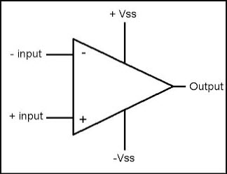
Comparator:
In electronics, a comparator is a device that compares two voltages or
currents and outputs a digital signal indicating which is larger. Given below is the comparator circuit device.
Flip Flop:
In electronics, a flip-flop or latch is a circuit that has two stable states and
can be used to store state information a bistable multivibrator. The IC of the Flip Flop is shown below
Transistor:
It is a semiconductor device used to amplify or switch electronic
signals and electrical
power.
The ICs of the transistor is given below
Output Inverter:
The key quality of the output inverter is that it will inverted the signal coming at the output..
The output inverter IC is given below.
Functions of the Pins:
There are total 8 pins on the 555 timer IC and each perform different function.
- Ground: This pin is used to provide a zero voltage rail to the Integrated circuit
to divide the supply potential between the three resistors shown in the
diagram.
- Trigger: As we can see that the voltage at the non-inverting end of the
comparator is Vin/3, so if the trigger input is used to set the output of the F/F
to ‘high’ state by applying a voltage equal to or less than Vin/3 or any negative
pulse, as the voltage at the non-inverting end of the comparator is Vin/3.
- Output: It is the output pin of the IC, connected to the Q’ (Q-bar) of the F/F
with an inverter in between
- Reset: This pin is used to reset the output of the F/F regardless of the initial
condition of the F/F and also it is an active low Pin so it connected to ‘high’
state to avoid any noise interference, unless a reset operation is required. So
most of the time it is connected to the Supply voltage
- Control Voltage: As we can see that the pin 5 is connected to the inverting
input having a voltage level of (2/3) Vin. It is used to override the inverting
voltage to change the width of the output signal irrespective of the RC timing
network.
- Threshold: The pin is connected to the non-inverting input of the first
comparator. The output of the comparator will be high when the threshold
voltage will be more than (2/3) Vin thus resetting the output (Q) of the F/F
from ‘high’ to ‘low
- Discharge: This pin is used to discharge the timing capacitors (capacitors
involved in the external circuit to make the IC behave as a square wave
generator) to ground when the output of Pin 3 is switched to ‘low’
- Supply: This pin is used to provide the IC with the supply voltage for the
functioning and carrying of the different operations to be fulfilled with the
555 timer.
Applications of 555 Timer IC:
The IC 55 timer is used in many circuits, for example One-shot pulse generator in
Monostable mode as an Oscillator in Astable Mode or in Bistable mode to produce
a flip/flop type action. It is also used in many types of other circuit for achievement
of various purposes for instance Pulse Amplitude Modulatin (PAM), Pulse Width
Modulation (PWM) etc.
References:


Comments
Post a Comment